Universal Instruments Corporation

Universal Instruments is a global leader in the design and manufacture of advanced automation and assembly equipment solutions for the electronics manufacturing industry.
With a lineage of more than 50 years, Universal is the longest-standing company in the electronics assembly space.
Universal provides complete solutions to meet specific requirements by leveraging its portfolio of flexible platforms for surface mount, through-hole, advanced semiconductor packaging, light mechanical, and final assembly processes. This best-in-class equipment set is complemented by state of the art software and operational services to help customers monitor and manage operational activities, improve efficiency and lower overall costs of manufacturing. Universal provides exclusive manufacturing process expertise through its world-renowned Advanced Process Lab, and delivers lasting value and support throughout all phases of the ownership experience through a global service infrastructure. Universal maintains offices in the Americas, Europe, and Asia, and is represented through a worldwide direct sales and distributor network.
For manufacturers who want to maximize return on investment for their electronics assembly solutions across the overall product life cycle, Universal Instruments delivers comprehensive, customer-focused solutions for all electronics production environments.
Leveraging innovative technologies and exclusive expertise, Universal solutions optimize time to market, overall efficiency for volume production, and investment protection for any product mix.
Universal Instruments Corporation Postings
3 products »
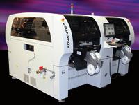
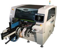
AdVantis - SMT Pick and Place Series
Flexible, Scalable Solutions For Maximum Versatility. Advantis® sets a higher standard for midrange assembly solutions, offering unmatched performance and flexibility at a low entry price. Advantis delivers scalable capacity, easy-...
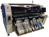
Fuzion SMT Pick and Place Series
Fuzion® is Universal’s flagship platform, leveraging the latest generation of head and feeder technologies, and software tools for maximum performance. Fuzion solutions maximize utilization, Overall Equipment Effectiveness (OEE), and...
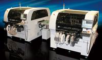
Genesis SMT Pick and Place Series
The ideal solution for any market. Genesis features a powerful combination of speed and flexibility to blur the boundaries between high-speed and flexible fine pitch placement. Outstanding price performance combines with traditional Un...
13 technical articles »
Solder Joint Reliability Under Realistic Service Conditions
Oct 30, 2014 | P. Borgesen, S. Hamasha, M. Obaidat, V. Raghavan, X. Dai; Department of Systems Science & Industrial Engineering, Binghamton University, M. Meilunas, M. Anselm; Universal Instruments Corporation.
The ultimate life of a microelectronics component is often limited by failure of a solder joint due to crack growth through the laminate under a contact pad (cratering), through the intermetallic bond to the pad, or through the solder itself. Whatever the failure mode proper assessments or even relative comparisons of life in service are not possible based on accelerated testing with fixed amplitudes, or random vibration testing, alone. Effects of thermal cycling enhanced precipitate coarsening on the deformation properties can be accounted for by microstructurally adaptive constitutive relations, but separate effects on the rate of recrystallization lead to a break-down in common damage accumulation laws such as Miner's rule. Isothermal cycling of individual solder joints revealed additional effects of amplitude variations on the deformation properties that cannot currently be accounted for directly.
We propose a practical modification to Miner's rule for solder failure to circumvent this problem. Testing of individual solder pads, eliminating effects of the solder properties, still showed variations in cycling amplitude to systematically reduce subsequent acceleration factors for solder pad cratering. General trends, anticipated consequences and remaining research needs are discussed...
Testing Intermetallic Fragility on Enig upon Addition of Limitless Cu
Jan 23, 2014 | Martin K. Anselm, Ph.D. and Brian Roggeman Universal Instruments Corp.
As reliability requirements increase, especially for defense and aerospace applications, the need to characterize components used in electronic assembly also increases. OEM and EMS companies look to perform characterizations as early as possible in the process to be able to limit quality related issues and improve both assembly yields and ultimate device reliability. In terms of BGA devices, higher stress conditions, RoHS compatible materials and increased package densities tend to cause premature failures in intermetallic layers. Therefore it is necessary to have a quantitative and qualitative test methodology to address these interfaces....
Process Issues For Fine Pitch CSP Rework and Scavenging
Mar 04, 2013 | Anthony A. Primavera Ph.D.
Chip-scale (or chip-size) packages are rapidly becoming an important element in electronics due to their size, performance, and cost advantages [Hou, 1998]. The Chip Scale Package (CSP) is becoming a key semiconductor package type, particularly for consumer products. Due to their relatively smaller size, new challenges are presented in the rework and repair of CSPs. (...) The specific focus of this paper is the removal process for rework of CSPs and the site scavenging methods required to properly prepare the circuit board for a new component. Process factors such as the heating, fluxing and, atmosphere are discussed....
Optimizing Flip Chip Substrate Layout for Assembly
Nov 29, 2007 | Pericles Kondos, Peter Borgesen, Dan Blass, and Antonio Prats.
Programs have been developed to predict the expected yield of flip chip assemblies, based on substrate design and the statistics of actual manufactured boards, as well as placement machine accuracy, variations in bump sizes, and possible substrate warpage. These predictions and the trends they reveal can be used to direct changes in design so that defect levels will fall below the acceptable limits. Shapes of joints are calculated analytically, or when this is not possible, numerically by means of a public domain program called Surface Evolver. The method is illustrated with an example involving the substrate for a flip chip BGA....
The Pin-in-Paste (or AART) Process for Odd Form and Through Hole Printed Circuit Boards
Sep 27, 2007 | Jay B. Hinerman, DEK Inc; K. Srihari, Ph.D., Department of Systems Science and Industrial Engineering State University of New York; George R. Westby, Director - SMT Laboratory, Universal Instruments Corporation.
Considerable interest exists in the process known as the pinin- paste, or the Alternative Assembly and Reflow Technology (AART) process. The AART process allows for the simultaneous reflow of both odd-form and through hole devices as well as surface mount components. This process has several advantages over the typical mixed technology process sequence that includes wave soldering and/or hand soldering, often in addition to reflow soldering....
Achieving SMT Compatible Flip Chip Assembly With No-Flow Fluxing Underfills
Aug 09, 2007 | Tony DeBarros and Doug Katze of Emerson and Cuming And Pericles Kondos of Universal Instruments
Recent developments in No Flow-Fluxing Underfill (NFFUF) products have demonstrated their utility to enhance the reliability of flip chip assemblies with reduced processing steps over conventional capillary flow methods. This basic work considered processing conditions such as dispensed volume and placement force, speed and dwell time. Further evaluations of these new products on a variety of flip chip assembly configurations manufactured by various processes have been undertaken to provide further evidence of their suitability and potential in high volume electronic manufacturing. This paper summarizes the recent evaluations and discusses new studies of additional assembly configurations, which include higher input/output (l/O) counts up to full arrays in excess of 1200 l/Os....
Low Force Placement Solution For Delicate and Low IO Flip Chip Assemblies
Jun 27, 2007 | Jason Higgins - Universal Instruments Corporation, Robert Hemann - Medtronic Microelectronics Center.
Traditionally most flip chips were designed with large bumps on a coarse pitch. However, as the trend towards smaller, more compact assemblies continues the sizes of semiconductor packages are forced to stay in line. New designs are incorporating smaller bump diameters on increasingly aggressive pitches, and in many cases decreasing the total IO count. With fewer and smaller bumps to distribute the load of the placement force it is becoming increasingly vital for equipment manufacturers to meet the challenge in offering low force placement solutions. One such solution will be presented in the following discussion. Also presented will be ways to minimize the initial impact spike that flip chips experience upon placement....
Lead-free and Tin-lead Assembly and Reliability of Fine-pitch Wafer-Level CSPs
May 31, 2007 | Michael Meilunas, Muffadal Mukadam, Peter Borgesen, Hari Srihari
This paper discusses solder paste printing and flux dipping assembly processes for 0.4 and 0.5mm pitch lead-free WLCSPs and the corresponding assembly results and thermal cyclic reliability obtained. Variables evaluated include reflow ambient, paste type, and stencil design. Reliability is also compared to results for the same components assembled under identical conditions using SnPb solder....
The Proximity of Microvias to PTHs And Its Impact On The Reliability
May 09, 2007 | Anthony Primavera Manager - CSP Consortium Universal Instruments Corporation, Jaydutt Joshi, Package Development Engineer - Conexant Systems Inc.
High Density Interconnect (HDI) technology is fast becoming the enabling technology for the next generation of small portable electronic communication devices. These methods employ many different dielectrics and via fabrication technologies. In this research, the effect of the proximity of microvias to Plated Through Holes (PTHs) and its effect on the reliability of the microvias was extensively evaluated. The reliability of microvia interconnect structures was evaluated using Liquid-To-Liquid Thermal Shock (LLTS) testing (-55oC to +125oC). Comprehensive failure analysis was performed on microvias fabricated using different via fabrication technologies....
Fragility of Pb-free Solder Joints
Apr 18, 2007 | Universal Instruments Corporation
Recent investigations have revealed that Pb-free solder joints may be fragile, prone to premature interfacial failure particularly under shock loading, as initially formed or tend to become so under moderate thermal aging. Depending on the solder pad surface finish, different mechanisms are clearly involved, but none of the commonly used surface finishes appear to be consistently immune to embrittlement processes. This is of obvious concern for products facing relatively high operating temperatures for protracted times and/or mechanical shock or strong vibrations in service....
3 more technical articles from Universal Instruments Corporation »
60 news releases »
Universal Appoints Technical Marketing Company to Represent its Advanced Process Lab
![]() Jun 07, 2020 | Universal Instruments' Advanced Process Lab (APL) is pleased to announce that it has appointed Technical Marketing Company (TMC) as its Channel Partner. Chris Dodd, President and principal owner, and the TMC team will represent Universal's APL throughout the Rocky Mountain region.
Jun 07, 2020 | Universal Instruments' Advanced Process Lab (APL) is pleased to announce that it has appointed Technical Marketing Company (TMC) as its Channel Partner. Chris Dodd, President and principal owner, and the TMC team will represent Universal's APL throughout the Rocky Mountain region.
GPD Global Installs Precision Dispenser at Universal’s Advanced Process Lab
![]() Dec 17, 2019 | Universal Instruments’ Advanced Process Lab (APL) is pleased to announce that GPD Global has placed a MAX II precision dispenser in its lab in New York. Universal’s APL offers comprehensive research, analytical and advanced assembly services that enable manufacturers to realize rapid product introduction, maximize yield and optimize reliability.
Dec 17, 2019 | Universal Instruments’ Advanced Process Lab (APL) is pleased to announce that GPD Global has placed a MAX II precision dispenser in its lab in New York. Universal’s APL offers comprehensive research, analytical and advanced assembly services that enable manufacturers to realize rapid product introduction, maximize yield and optimize reliability.
Universal Showcases Surface Mount and Odd-Form Capabilities at IPC APEX
![]() Feb 06, 2018 | Universal Instruments will feature flexible surface mount, odd-form and automation platform solutions at the 2017 IPC APEX EXPO held at the San Diego Convention Center on February 27 – March 1. On booth 3141, Universal will demonstrate its FuzionOF™ high-speed automation platform, extra-capacity FuzionXC2-37™ Platform and Uflex™ modular automation platform.
Feb 06, 2018 | Universal Instruments will feature flexible surface mount, odd-form and automation platform solutions at the 2017 IPC APEX EXPO held at the San Diego Convention Center on February 27 – March 1. On booth 3141, Universal will demonstrate its FuzionOF™ high-speed automation platform, extra-capacity FuzionXC2-37™ Platform and Uflex™ modular automation platform.
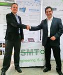
Universal Welcomes SMTo Engineering to Channel Partner Network
![]() Jul 06, 2017 | Universal Instruments has enriched its customer coverage in Mexico with the addition of a new Channel Partner, SMTo Engineering S.A. de C.V. SMTo Engineering complements Universal’s Customer Operations infrastructure in the territory by leveraging a thorough understanding of the Mexican market to provide best-in
class technology solutions in the form of capital equipment, as well as consumables and engineering services for peripheral electronics assembly process equipment.
Jul 06, 2017 | Universal Instruments has enriched its customer coverage in Mexico with the addition of a new Channel Partner, SMTo Engineering S.A. de C.V. SMTo Engineering complements Universal’s Customer Operations infrastructure in the territory by leveraging a thorough understanding of the Mexican market to provide best-in
class technology solutions in the form of capital equipment, as well as consumables and engineering services for peripheral electronics assembly process equipment.
Wistron and Universal Instruments Building Successful Alliance
![]() Mar 08, 2017 | Taiwan-based EMS, Wistron Corporation continues to successfully adapt to its evolving customer product portfolio with a manufacturing model that includes Universal Instruments’ Fuzion Platform. Wistron has now integrated more than 60 Fuzion, including several platforms purchased earlier this year, to perform complex odd-form applications while maintaining a 99.9% yield for volume production of information and communication technology (ICT) products
Mar 08, 2017 | Taiwan-based EMS, Wistron Corporation continues to successfully adapt to its evolving customer product portfolio with a manufacturing model that includes Universal Instruments’ Fuzion Platform. Wistron has now integrated more than 60 Fuzion, including several platforms purchased earlier this year, to perform complex odd-form applications while maintaining a 99.9% yield for volume production of information and communication technology (ICT) products
Universal Appoints Jeff Knight General Manager, APL and Advanced Technology Assembly Services
![]() Jul 21, 2016 | Universal Instruments is pleased to announce the appointment of Jeff Knight as General Manager of the Advanced Process Lab (APL) and Advanced Technology Assembly Services (ATAS). Knight will operate out of the company’s corporate headquarters in Conklin, NY and will be responsible for generating new business opportunities for Universal’s advanced technology groups at both the Conklin and Rochester, NY facilities while also ensuring an exceptional level of support and success for the existing customer base.
Jul 21, 2016 | Universal Instruments is pleased to announce the appointment of Jeff Knight as General Manager of the Advanced Process Lab (APL) and Advanced Technology Assembly Services (ATAS). Knight will operate out of the company’s corporate headquarters in Conklin, NY and will be responsible for generating new business opportunities for Universal’s advanced technology groups at both the Conklin and Rochester, NY facilities while also ensuring an exceptional level of support and success for the existing customer base.
![]() Feb 18, 2016 | EEI Manufacturing Services announced September 29th 2015 that the Department of the Navy has approved a 33-month $2.24 million Mentor-Protégé agreement between Raytheon Space and Airborne Systems (SAS) and EEI Manufacturing Services.
Feb 18, 2016 | EEI Manufacturing Services announced September 29th 2015 that the Department of the Navy has approved a 33-month $2.24 million Mentor-Protégé agreement between Raytheon Space and Airborne Systems (SAS) and EEI Manufacturing Services.
Universal's APL to Deliver Technical Session at LED A.R.T. Symposium
![]() Nov 14, 2015 | Denis Barbini, PhD, Associate Director of Universal Instruments’ Advanced Process Lab (APL), will present a technical session entitled LED Electronics – A Guide to Developing a Manufacturing Process at the LED Assembly, Reliability & Testing (A.R.T.) Symposium in Atlanta, GA on November 17–19, 2015. The presentation will examine key considerations for the design and manufacturing of LED products, driven by research performed by the APL.
Nov 14, 2015 | Denis Barbini, PhD, Associate Director of Universal Instruments’ Advanced Process Lab (APL), will present a technical session entitled LED Electronics – A Guide to Developing a Manufacturing Process at the LED Assembly, Reliability & Testing (A.R.T.) Symposium in Atlanta, GA on November 17–19, 2015. The presentation will examine key considerations for the design and manufacturing of LED products, driven by research performed by the APL.
Universal Features Surface Mount and Automation Solutions at Productronica 2015
![]() Nov 01, 2015 | Universal Instruments will demonstrate both its high-speed flexible Fuzion1-30™ and ultra-flexible Fuzion1-11™ platforms at Productronica 2015, held November 10–13 at the Munich Trade Fair Center, Germany. Complementing these solutions on the booth will be the Polaris Assembly Cell, offering cost-effective performance for extreme odd-form automation and light mechanical assembly applications. Universal will exhibit on Hall A2, Booth 459 in cooperation with channel partner, smartTec GmbH.
Nov 01, 2015 | Universal Instruments will demonstrate both its high-speed flexible Fuzion1-30™ and ultra-flexible Fuzion1-11™ platforms at Productronica 2015, held November 10–13 at the Munich Trade Fair Center, Germany. Complementing these solutions on the booth will be the Polaris Assembly Cell, offering cost-effective performance for extreme odd-form automation and light mechanical assembly applications. Universal will exhibit on Hall A2, Booth 459 in cooperation with channel partner, smartTec GmbH.
Universal Fortifies Americas Operations, Appoints Michael Welch Regional Manager
![]() May 07, 2015 | Industry experience and technical expertise enriches Universal’s ability to exceed customer expectations in US southern states.
May 07, 2015 | Industry experience and technical expertise enriches Universal’s ability to exceed customer expectations in US southern states.
50 more news releases from Universal Instruments Corporation »
